The semiconductor industry is foundational to modern technology, driving advances in computing, telecommunications, and a myriad of other sectors. A critical component of semiconductor manufacturing is the use of nitrogen (N2) gas. Due to its inert nature, nitrogen plays a pivotal role in various stages of semiconductor production, ensuring the quality and reliability of electronic devices. This article delves into the multifaceted applications of nitrogen in the semiconductor industry, highlighting its importance in maintaining the integrity of manufacturing processes.
Nitrogen in Cleaning and Etching
Cleaning and etching processes are essential for preparing semiconductor surfaces for further manufacturing steps. Nitrogen is extensively used as a carrier gas, mixed with reactive gases, to clean or etch silicon wafers. Its inertness ensures that no additional contaminants are introduced during these processes, which is crucial for maintaining the purity of semiconductor materials. For example, in plasma etching, nitrogen helps stabilize reactive plasma, enabling precise control over the etching process.
CVD and PVD
Nitrogen’s application extends to Chemical Vapor Deposition (CVD) and Physical Vapor Deposition (PVD) techniques. These processes involve depositing thin film materials onto semiconductor wafers to form various components of electronic devices. Nitrogen, acting as a carrier gas in CVD processes, ensures the transport of precursor gases to the wafer surface. In PVD processes, nitrogen may be used to create a reactive atmosphere that aids in the formation of specific types of films, such as nitrides, which are essential for semiconductor devices.
Creating an Inert Atmosphere
The semiconductor manufacturing environment demands stringent control over atmospheric conditions to prevent oxidation and contamination. Nitrogen gas is employed to create an inert atmosphere in wafer fabrication and assembly areas. This controlled environment is essential for processes such as annealing, where the presence of oxygen can adversely affect the material properties of the semiconductors.
Semiconductor Packaging
Packaging is the final step in semiconductor device fabrication, involving the encapsulation of chips to protect them from physical and chemical damage. Nitrogen is used to purge oxygen and moisture from the packaging environment, preventing corrosion and ensuring the longevity of the semiconductor devices. The use of nitrogen in this stage underscores its role in enhancing the durability and reliability of electronic components.
Temperature Control Applications
In addition to its role as a protective gas, nitrogen is also utilized for temperature control during semiconductor manufacturing. Due to its thermal properties, nitrogen can be used to manage the temperature of wafers during processes that require precise thermal management, such as rapid thermal annealing. This application of nitrogen ensures that thermal treatments are uniform, which is vital for the consistent quality of semiconductor devices.
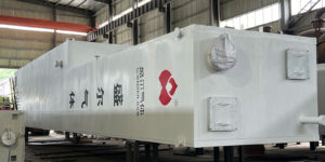
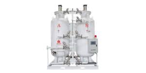
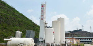
The application of nitrogen in the semiconductor industry is integral to the production of high-quality, reliable semiconductor devices. Its inert nature and versatile properties make nitrogen an indispensable resource across various manufacturing stages, from cleaning and etching to deposition, atmosphere control, packaging, and temperature management. As the semiconductor industry continues to evolve, the demand for nitrogen and advanced air separation technologies is expected to grow, nitrogen generators are becoming more and more important in the semiconductor industry.